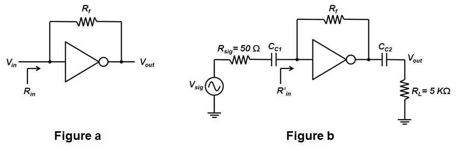
2. Perform a small signal AC analysis on the circuit in Figure-a to find an expression for Rin and Ao=Vout/Vin. Use the Pi model for NMOS and PMOS and simplify the circuit before you start writing the equations. Consider Gm = gm_n + gm_p and Ro = ro_n || ro_p.
3. Perform a small signal AC analysis on the circuit in Figure-b to find an expression for the overall voltage gain, Av=Vout/Vsig. Use the results from step 2 to find Av. Hint: The effective input voltage in Figure-b can be calculated using a voltage division between Rsig and R'in. Also, R'in is a similar expression to Rin, except that R'o will be Ro || RL. Similarly, A'o is a similar expression to Ao, except that R'o will be Ro || RL.
4. Now assume that the parameters for the inverter are as follows. The NMOS parameters are K'n=100 uA/V2, VTn=1.2 V, Lambda=0.01 V-1 and (W/L)n=(25um/0.25um). The PMOS parameters are K'p=60 uA/V2, VTp=-1.0 V, Lambda=0.01 V-1 and (W/L)p=(31.3um/0.25um).
5. Perform a DC analysis to find DC operating point of the circuit in Figure-a, using the inverter transistor parameters provided in 4. This analysis is similar to finding the switching threshold voltage of the inverter. Calculate ID, VOV, gm, and ro of NMOS and PMOS.
6. Using the transistor parameters found in 5 and the expression for the overall voltage gain found in 3, calculate the resistance of the feedback resistor, Rf, such that the overall mid-band gain becomes -60. You will need to solve the equation numerically. Note that at mid-band frequencies, both Cc1 and Cc2 are shorted.
7. Determine which coupling capacitor (Cc1 or Cc2) is associated to the dominant pole for low frequency. Set 10 Hz for the dominant and 1 Hz for the non-dominant poles to calculate Cc1 and Cc2.
8. Estimate the high frequency poles assuming Cgs_n=Cgs_p=1 pF and Cgd_n=Cgd_p=0.25 pF. Then estimate the higher 3-dB frequency, fH, for this amplifier. Specify the node that causes the dominant pole.
9. Determine the maximum output voltage swing (Vout_min and Vout_max) for your amplifier.
10. Calculate the DC power consumption of your amplifier.
11. Simulate your amplifier using TSPICE and compare your hand calculations with simulation results for gain, power consumption, lower 3-dB and higher 3-dB frequencies. Enter the simulated, calculated, and %errors for each in a table.
12. perform a transient analysis in TSPICE to demonstrate the maximum output swing (Vout_min and Vout_max)., for a sine wave input signal.
13. Explain the pros and cons of this non-conventional amplifier design.
14. One design with the most comprehensive analysis and report will receive 10% bonus credit for this project.