

Semester Project:
Goal
The goal of this project is to design and layout a 1-bit digital comparator. Digital comparator are widely used in digital electronics circuits. In this project you are asked to design, layout, and charterize a basic 1 bit digital comparator.
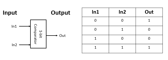
The block diagram of the comparator is given below. When both the inputs In1and In2 are same then the output terminal go to logic "high" or '1' otherwise it go to logic "low" or "0". The truth table for the 1-bit comparator is given below. In this project, student are required to design the 1-bit comparator that is optimized for power, delay and/or area.
Design Requirement
1. The student will form groups of no more than two for this project. Make sure that the work is divided equally between the members of each group
2. There are many ways that you can implement a comparator. Check online resources and select one type of comparator that you think can provide the best power, area, or delay tradeoff.
3. Download the Ledit file from here. Please make sure not to alter the ON_C5N.ext and design rule in the ledit file.
4. Your design is required to be DRC clean. If its not DRC clean then I will consider it as incomplete.
5. Once the extracted SPICE file is created, use the ON_C5N.modlib that defines the MOSFETs and then perform the simulations by adding input sources and commands to the extracted SPICE file.
6. Provide a clean schmatic drawing for your report
7. Use 1.8V power supply and a 10fF load capacitor in the output for your spice simulations.
Due Date
The complete report is due in class on Thursday, 23rd of July, 2015.
Deliverables
A written report that contains but not limited to the following items.
1. Give some brief explanation on how you designed the multiplexer (for example, schematic, logic style, sizing, etc).
2. Complete layout with X and Y dimensions and the total area.
3. Original SPICE file (circuit netlist). In your PSPICE file, make sure to include AS, AD, PS, and PD for each transistor based on your layout.
4. Waveforms from PSPICE simulations that shows the functionality of the multiplexer. Clearly show all the data (inputs and outputs) on the waveforms.
5. Using SPICE, measure the worst case switching energy and the worst case delay of the comparator. Use a 10fF load capacitor in your energy and delay measurement in the PSPICE simulation. Assume the input rise time is very fast (10ps or less).
6. Summarize your layout area, measured switching energy, and measured delay in a table.
7. Again using PSPICE, measure the output resistance and the input capacitance of In1 and In2 in your comparator. Use a 1pF load capacitor and a 10KOhm series resistor for your output and input cell characterization.
8. Summarize the cell characterization values (Rout, Cin(In1), and Cin(In2)) in a table.
9. A table showing the hour spent for each task by each member of the group.