ECE
520/424 - VLSI Design: Spring 2026
University of New Mexico
Goal:
The
goal of this project is to design and layout a CMOS random bit
generator chip. The design should be optimized for robustness,
power, and/or area. The
project will consist of two phases. In
the first phase, the schematic of the project will be designed, and the
functionality must be verified using SPICE simulations.
Students
must form groups of three/four students per group for this project.
Make sure that the work is divided equally between the members of each
group.
In the second phase, the layout of the random bit generator chip
will be finished without any DRC violation. Due to the tool's
limitation, there is no need to extract the layout for further
verification.
Design Requirements:
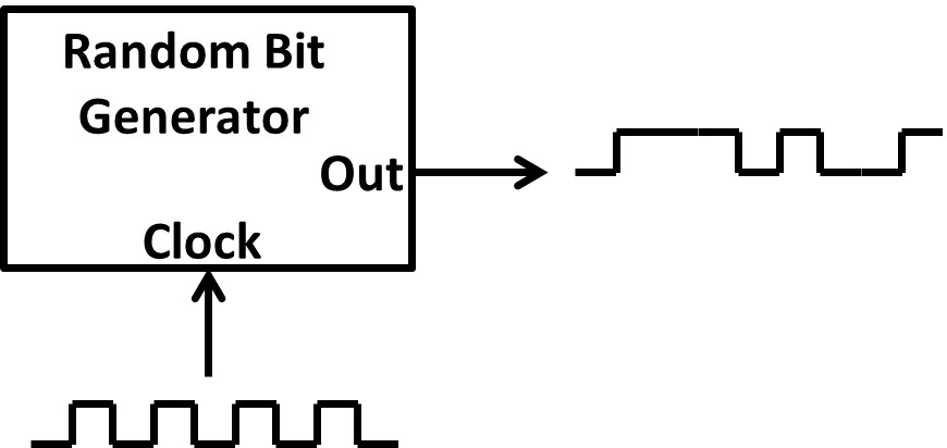
1. Random
bit generator circuits generates unpredictable random bits at a
specific clock frequency, which is the central part of several
applications, such as cryptographic systems and hardware security. In
this project, we will be designing a 1-bit random signal at the rising
edge of each clock pulse. Feel free to use any online resources and
choose a technique you prefer, including PRBS or noise-based
methods. The goal of this project is to submit the design for tape
out and fabricate the test chips using 0.5um ON Semiconductor.
In your design consider the robustness, area, testability, and
functionality from the beginning of the design. If
possible, we may submit one design to MOSIS for manufacturing. The
group that
is chosen for fabrication (the best functionality, testability, and
robustness) will obtain 10% bonus credit for the project.
2. Design
and test each block individually. Combine the blocks once you confirm
the simulation results for each block.
3.
Use wide metal layers for the VDD and GND lines.
4. Please
download the pad frame file, ON_5CN_Pads.tdb,
for your project. Please design your layout in a new cell and
instantiate the pad frame on your top cell. The Pad_Frame cell has been
locked to prevent any accidental edits.
5. The
pad frame that has been created for you in this file, consists of 30
I/O and one GND and one VDD pads. The VDD pad is located on the right
and GND pad is located on the left of the frame. The I/O pad terminals
are labeled as DATA and is on Metal 2, but the VDD and GND pad
terminals are in Metal 1.
6. The
I/O pads are all the same, with only ESD protection devices. You can
simply use it as an input, but if you want to use it as an output, you
need to design appropriate driver for it. Consider 1 pF load for the
regular output pads.
7. For
SPICE simulations, please download the SPICE
model for
0.5 um ON Semiconductor CMOS process. Using S-Edit is not required for
this project, but a schematic must be presented in your reports.
8. The
L-Edit file contains all the DRC rules. However, the design rules can
be also found here (SCMOS_SUBM
column). In this process, Lambda is set to be 0.3um in the L-Edit setup
file.
9. Make
sure to have a plan for diagnosis. If your chip doesn't work, how can
you debug and identify the problem?
10.
Follow the naming convention and input output characteristics as below.
Our spec for maximum clock frequency is 5MHz. Therefore, make sure that
your maximum delay or rise/fall time is less than 10ns.
Item
|
Pins
|
Descriptions
|
Input
|
Data, Clock
and Reset
|
Input
capacitance should not cause more than 50fF load to its previous stage.
|
Output
|
Random Bit
|
Output ports
should have loads of 1pF when performing simulation
|
Supply
voltage
|
VDD and GND
|
5.0 V
|
Due Dates:
Phase
one: schematic and SPICE simulation results due on Thursday April 16,
2026
Phase two: layout and post-layout simulations due on Thursday May
7, 2026
Deliverables:
A
written report that contains but not limited to the following items.
Only electronic copies for the project reports are accepted. Please
email your report (pdf) and related files to me (pzarkesh@unm.edu) on
the due date.
1. The schematic and associated SPICE file (circuit netlist).
2. Give some bullet points explaining how you designed each block (for
example, schematic, logic style, sizing, etc).
3. Waveforms from simulations on each block independently. Clearly show
all the data (inputs and outputs) on the waveforms.
4. Waveform that shows the functionality of the random bit generator.
Using SPICE, measure the rise and fall time of the output.
(5-10 applies to phase two only)
5. Brief explanation on your circuits (circuit type, optimization, and
changes since phase1)
6. Layout (.tdb file)
7. DRC reports showing there are no violations
8. A brief description of testing
strategy. How would you test your test chip after it will be
manufactured.
9. A table showing the hour spent
for each task by each member of the group.
10. E-mail your layout (.tdb) with your final report.